Our strength is in designing and manufacturing products that combine semiconductor and optical technology.
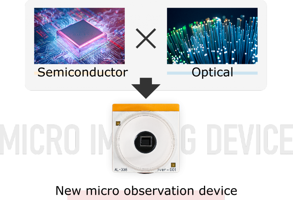
Semiconductor processing and functions have a potential to exceed the limits of existing optical technologies.
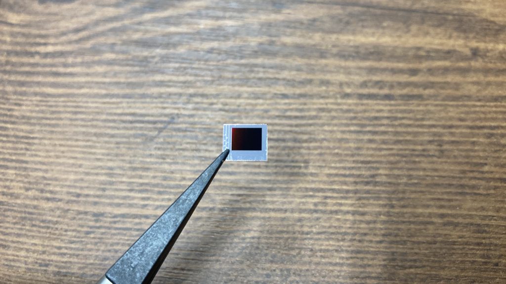
Taking advantage of these strengths, Soichiro Ueno, our founder, developed the Micro Imaging Device (“MID”).
A technology to do microscopic observation just by placing a sample on a chip of semiconductor, which arranges light-sensing elements in a fine mesh shape.
Microscopic observation can be performed in environments such as underwater and space, etc. where conventional microscopes were difficult to reach due to physical, climatic, or technical restrictions.
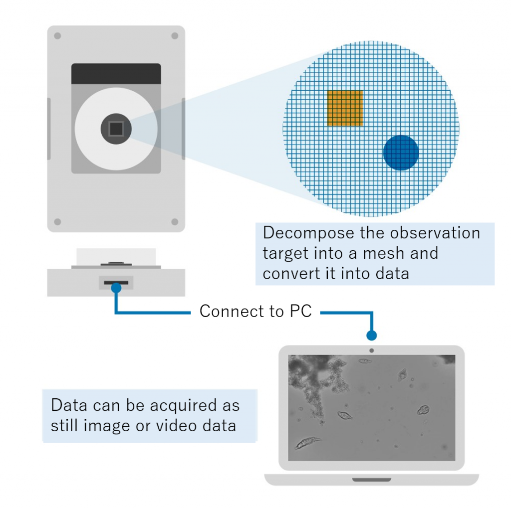
Microscopic observation can be performed easily without complicated operations such as focusing.
“Features of MID” alignment
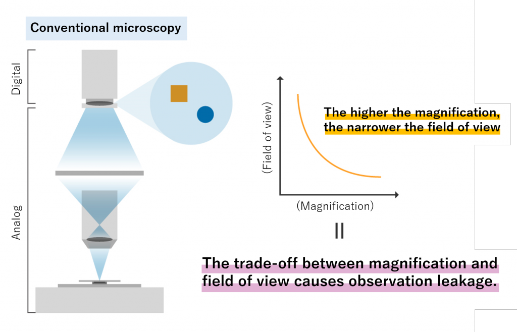
There is no trade-off between the field of view and the magnification because it does not use a lens. A wide field of view can be observed with high resolution.
Application example of MID” alignment
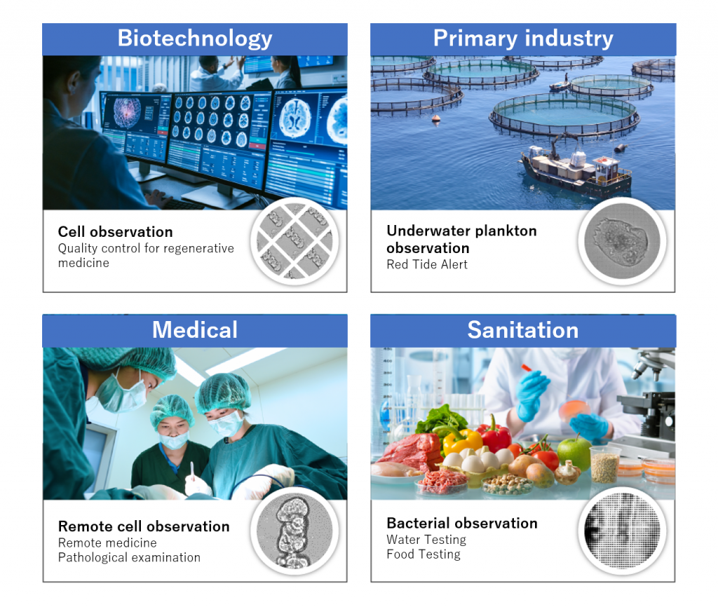
- Observation of cells and microorganisms in a general environment
- Observation of cells and microorganisms in water
- Microscopic observation in space